Fiber optic communication works by modulating a light source to encode information. The light travels through an optical fiber to a photodetector that converts it back into an electrical signal.
The key components of this process are:
- Optical source: A device that converts an electrical signal into modulated light. Common sources are light-emitting diodes (LEDs) and laser diodes.
- Optical fiber: A thin, flexible strand of glass or plastic that channels light using the principle of total internal reflection.
- Photodetector: A semiconductor device that absorbs light and generates an electrical current proportional to the optical power.
All these components rely on semiconductors – materials like silicon, gallium arsenide, and indium phosphide whose electrical conduction can be precisely controlled by doping. Understanding semiconductor physics is crucial for optical communication.
Table of Contents
Semiconductor Diode
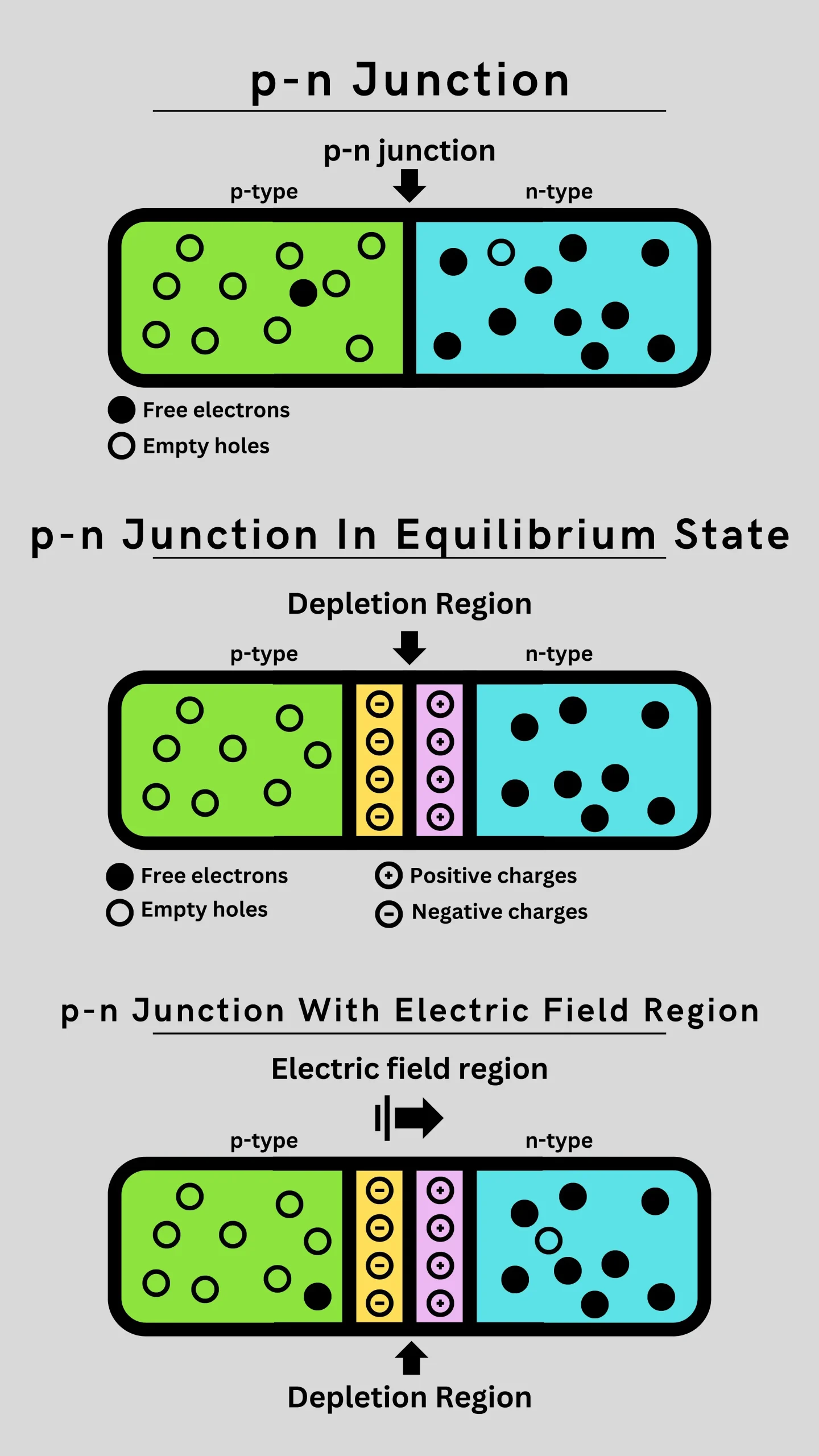
A semiconductor diode contains a p-n junction – a boundary between positively doped (p-type) and negatively doped (n-type) regions.
- In n-type regions, electrons are the majority carriers. In p-type regions, holes are the majority carriers.
- At equilibrium, diffusion of carriers across the junction leaves behind fixed ions, creating a depletion region that acts as an insulator.
- By applying a forward bias voltage, the depletion region shrinks, and electrons can flow across into empty holes, allowing current.
- A reverse bias widens the depletion region, blocking current flow. However, beyond a breakdown voltage, the diode conducts heavily in reverse.
Semiconductor diodes display a strong nonlinear current-voltage relationship that makes them incredibly useful. The p-n junction forms the basis for optical source and detector elements.
Bandgap Energy
Semiconductors contain allowed energy bands that electrons can occupy. The valence band is the highest occupied band at low energy. The next higher conduction band is initially empty.
Bandgap energy refers to the gap between the top of the valence band and the bottom of the conduction band. It represents the minimum energy needed to excite electrons from the valence band into the conduction band, where they can conduct electricity.
- Insulators have a large bandgap (> 4eV) that prevents conduction.
- Metals have overlapping bands, so electrons can freely move.
- Semiconductors like silicon and gallium arsenide have a small bandgap (1.1eV and 1.42eV, respectively) that allows conduction control.
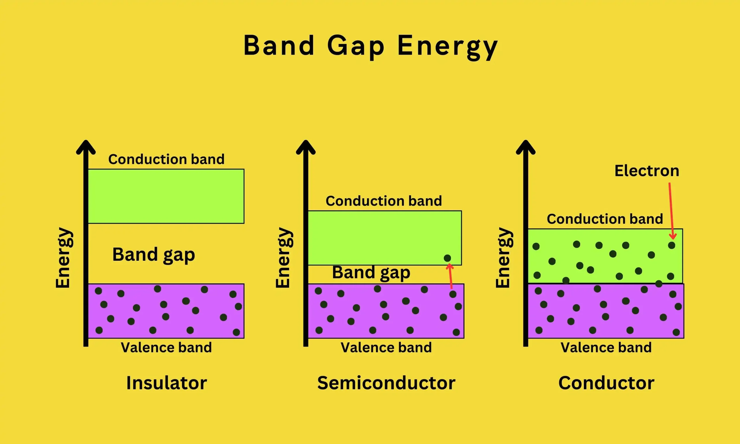
The bandgap represents the threshold energy for light emission in optoelectronic devices. Electrons decaying across the bandgap can emit photons instead of heat. Smaller bandgaps emit lower energy photons in the infrared, while larger bandgaps emit higher energy visible light.
P-N Junction
The p-n junction forms the basic building block of semiconductor devices. It contains adjacent p-type and n-type doped regions.
Depletion region
- At the junction interface, diffusion of carriers leaves behind fixed ions of opposite charge.
- This creates a depletion region with no mobile charges that acts as an insulator.
- Applying a reverse bias widens the depletion region by pulling apart carriers.
Biasing
- Under forward bias, the p-side is connected to the positive terminal and the n-side to the negative.
- This reduces the depletion width and allows current flow as electrons enter empty holes.
- A cutoff voltage of ~0.7V overcomes the built-in junction potential before conduction begins.
- In reverse bias, the voltage polarity is reversed. The depletion region widens, preventing current.
Breakdown
- At high reverse bias beyond the breakdown voltage, the strong field causes junction electrical breakdown.
- Junction resistance falls dramatically as avalanche carriers enable high reverse conduction.
Recombination
- Electrons entering the p-type region recombine with holes in the valence band.
- Recombination energy is emitted either as heat or light photons.
- Forward biasing enables light-emitting diodes and lasers.
The p-n junction’s versatile properties, such as nonlinear I-V characteristics, ability to emit light, and photodetection capabilities, enable a wide range of optoelectronic devices.
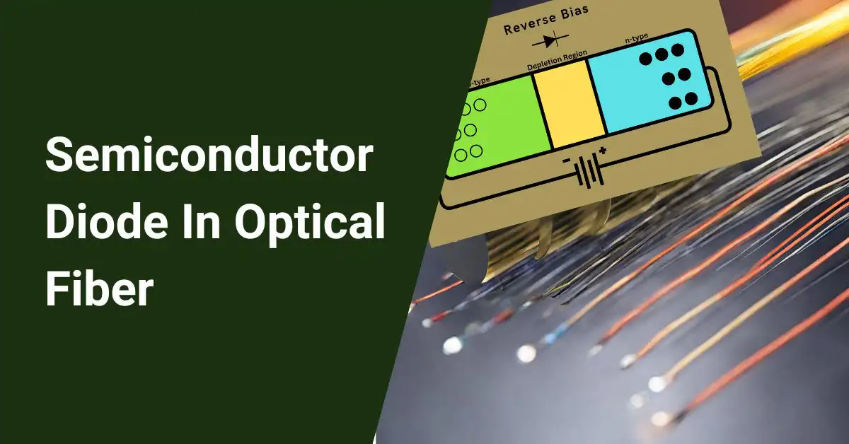
Reverse Bias
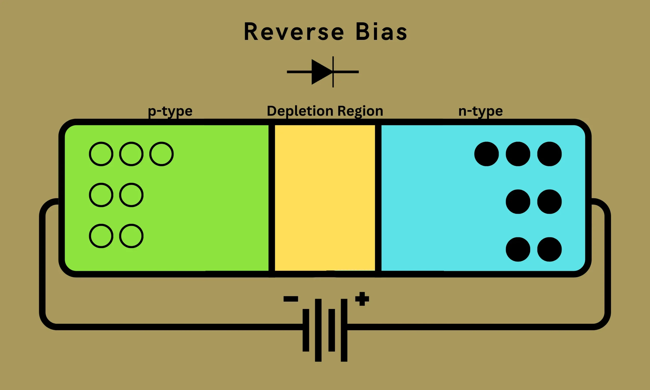
In a p-n junction under reverse bias, the p-type side is connected to the negative terminal of a voltage source, while the n-type side is connected to the positive terminal.
This bias:
- Widens the depletion region as electrons and holes move away from the junction.
- Increases the electric field strength across the depletion zone.
- Limits only a small leakage current due to minority carrier diffusion.
As the reverse voltage increases:
- The depletion width increases.
- The electric field strength keeps rising.
At the breakdown voltage (typically tens to hundreds of volts):
- The strong electric field accelerates carriers to high energies.
- This causes avalanche multiplication, leading to rapid junction conduction.
- Current rises suddenly as the p-n junction electrically “breaks down”.
Reverse bias forms the operating mode of photodetectors and solar cells. The high resistance allows a buildup of photo-generated current.
Forward Bias
Under forward bias, the p-type side of the diode is connected to the positive terminal of the supply, and the n-type side is connected to the negative terminal.
This bias:
- Reduces the depletion region width as minority carriers are injected across the junction.
- Allows electrons and holes to flow across the junction, enabling high conduction.
However, a minimum cut-in voltage of ~0.7V overcomes the built-in potential of the diode before appreciable conduction begins.
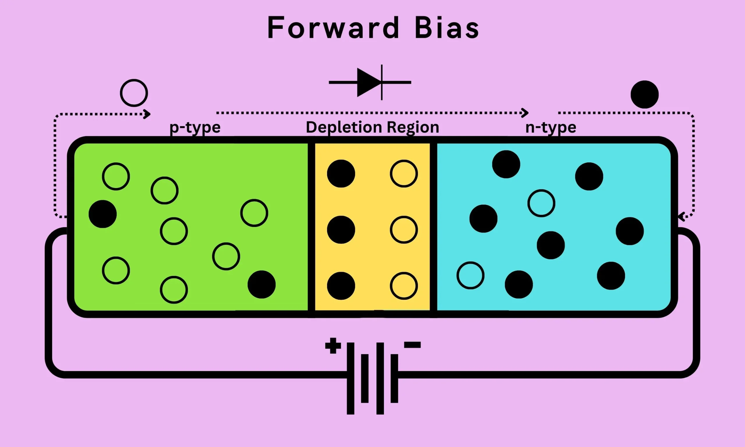
Once this cut-in voltage is exceeded:
- Forward current rises exponentially as the depletion region narrows.
- Electrons entering the p-type region recombine with holes, producing photons if the transition is radiative.
Forward bias enables LED and laser operation. The injected current causes conductive band electrons to combine with valence band holes radiatively.
Current-Voltage Characteristics
The current through a p-n junction diode varies nonlinearly with the applied voltage. This nonlinear I-V curve is a key diode characteristic.
Reverse bias:
- Very little current flows as the depletion region blocks conduction.
- At the breakdown voltage, the current increases suddenly due to avalanche breakdown.
Forward bias:
- Negligible current until the cut-in voltage (~0.7V for Si) is reached.
- Above this, the current increases exponentially as the depletion width shrinks.
The I-V curve displays a very sharp transition between reverse and forward conduction modes, as shown in the figure below:
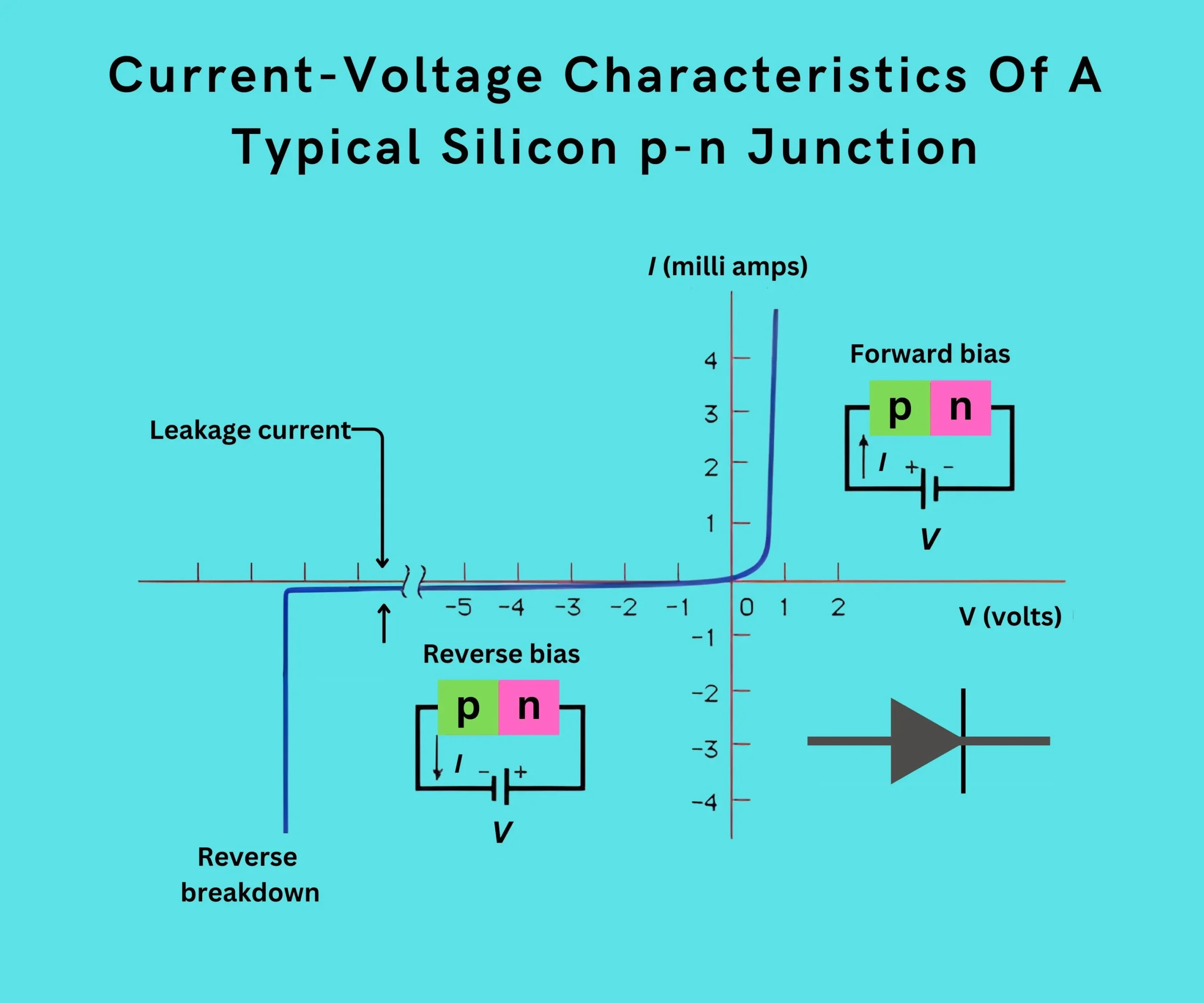
This nonlinear behavior makes diodes excellent current rectifiers and switches, enabling many optoelectronic applications.
Emission of Light
When forward-biased, electrons entering the p-type material recombine with holes in the valence band. Recombination energy is released either as heat or light.
Radiative recombination involves electron transitions that generate photons, causing light emission. Some ways this can occur:
- Spontaneous emission – Electrons randomly decay, emitting photons with random phases and directions.
- Stimulated emission – Incident photons trigger synchronous electron decay, generating coherent photons. This enables lasers.
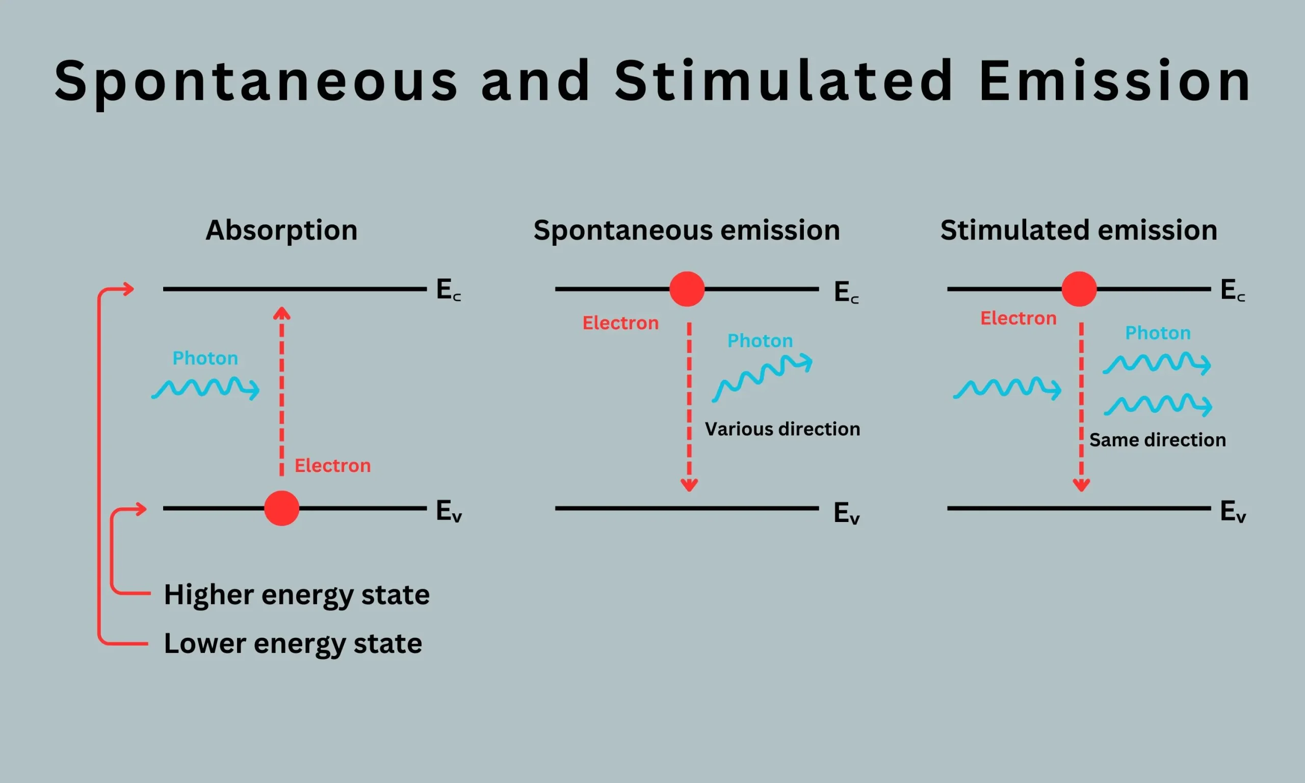
Non-radiative recombination converts electron-hole recombination energy into lattice vibration or heat without light emission.
The semiconductor’s bandgap energy determines the photon emission wavelength. Smaller bandgaps (e.g., 1 eV for Si) emit longer infrared wavelengths, while larger bandgaps (3.1 eV for GaAs) emit shorter wavelength visible light.
Light Sources for Fiber Optic Communication
For fiber optic communication, we need light sources that can convert electrical signals into optical signals. The light energy can originate from different sources:
- Heat – Heating a tungsten filament in an incandescent bulb causes it to emit light. However, these bulbs are inefficient and unsuitable for fiber optics.
- Electrical Discharge – Applying a high voltage to certain gases like neon or mercury vapor generates light emission. But gas discharge lamps aren’t easily controllable.
- Electric Current – When current flows through a semiconductor diode, electrons can recombine with holes and release energy as photons or light particles. This process enables light emitting diodes (LEDs) and laser diodes which are commonly used in fiber optics.
- Bioluminescence – Some animals like fireflies, naturally produce light through chemical reactions. While fascinating, these aren’t practical light sources for communication systems!
Now, let’s look at some semiconductor light emitters suited for optical fiber links:
- Light-Emitting Diodes (LEDs) – LEDs produce incoherent light when electrons recombine with holes in a forward-biased p-n junction. They are low cost, but output power is limited.
- Laser Diodes – These generate coherent light using the process of stimulated emission in a semiconductor laser cavity. Different types like Fabry-Pérot (FP), Distributed Feedback (DFB), and Vertical-Cavity Surface-Emitting Lasers (VCSELs) are used. Lasers offer high power and modulation speeds.
So, in summary, LEDs and laser diodes enabled by semiconductor physics are the most commonly used controllable light sources for optical communication using fiber optic cables. Their compact size and direct modulation capability make them perfect for fiber optic transmitters.
Conclusion
- Semiconductors like silicon and gallium arsenide enable precise control over electrical conduction using doped p-type and n-type regions.
- A p-n junction forms where p-type and n-type semiconductor regions meet. The nonlinear current flow through the junction is key.
- Forward biasing the junction enables LEDs and laser diodes to emit light. Reverse biasing enables photodetectors to sense light.
- Bandgap energy represents the minimum photon energy needed to excite electrons from the valence band to the conduction band.
- Small bandgaps (like silicon’s 1.1eV) emit infrared light. Wider bandgaps (e.g. 1.42eV for GaAs) emit visible wavelengths.
- Stimulated emission causes incident photons to trigger synchronous emission of identical photons from electron transitions. This optical amplification enables lasers.
In summary, semiconductor physics enables the transforming of electrical signals into modulated light by controlling electron energies and recombination. Optical communication relies on these fundamental principles to transmit information over fiber optic links.
FAQ
Which semiconductor device is used in optical communication systems?
Semiconductor laser diodes are the most common type of light source used in optical communication systems. They convert electrical current directly into light efficiently and reliably.
What are the advantages of semiconductor laser diodes in fiber optic communication?
➤ High efficiency: They convert most of the electrical energy into light, reducing power consumption.
➤ Compact size: Their small size allows for dense integration in communication equipment.
➤ Modulation capability: Their output intensity can be easily modulated to carry information.
➤ Wavelength range: They offer a wide range of operating wavelengths, accommodating different fiber types and applications.
What materials are in a semiconductor diode?
Semiconductor diodes typically use materials like Gallium Arsenide (GaAs), Indium Phosphide (InP), or Silicon (Si), depending on the desired operating wavelength and other properties.
What is the semiconductor optical amplifier (SOA)?
SOAs are semiconductor devices that amplify optical signals directly without converting them to electrical signals first. They offer advantages in high-speed data transmission and signal regeneration.
What are the limitations of semiconductor laser diodes?
One major limitation is temperature sensitivity: their performance can degrade with changes in temperature, requiring temperature control measures. Additionally, they generally offer lower output power compared to some other light sources like fiber lasers.
What are the emerging applications of semiconductor diodes in optical fibers?
➤ Biomedical sensors: Miniature sensors using these diodes can be used for minimally invasive medical procedures.
➤ Quantum communication: Certain types of diodes are crucial for generating and manipulating entangled photons for secure quantum communication.
➤ LiDAR: They play a key role in LiDAR systems for autonomous vehicles and 3D mapping.


